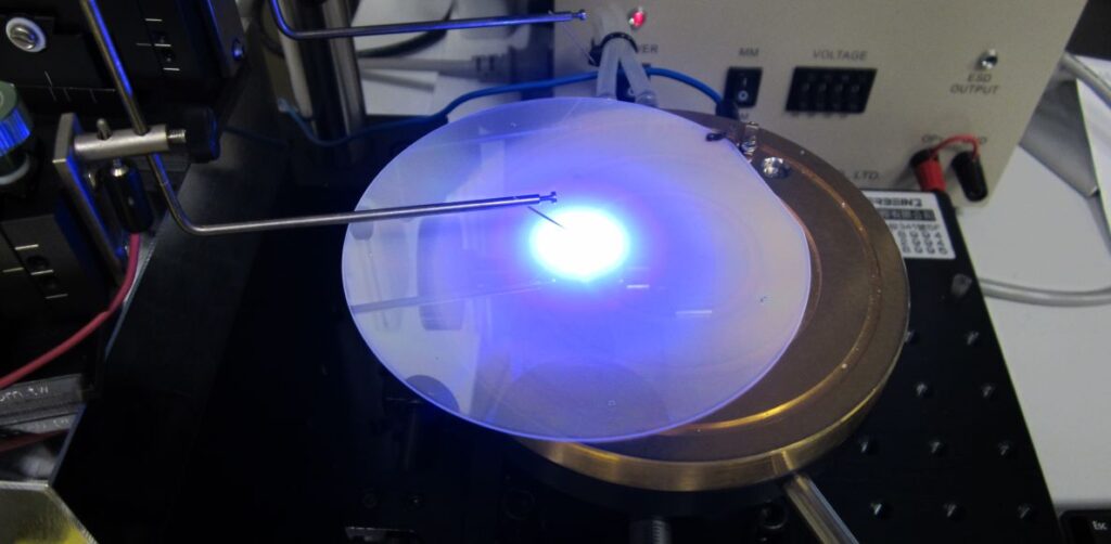
We provide Epitaxial Wafer design and growth service with our experience of more than 15 years. Our service covers different types of semiconductor device materials such as GaN, GaAs and InP. LEDs, Laser diodes, detectors, sensors, transistors and Integrated Circuits, solar cells and many other semiconductor, thin film and MEMS devices are uses these substrates as a base material.
Find Out More @ EPITAXIALWAFERS.COMGaN Based Epitaxial Wafers
- RF HEMT Epitaxial Wafers
- Power HEMT Epitaxial Wafers
- Visible LED Epitaxial Wafers
- 275nm DUV LED Epitaxial Wafers
- AlN Templates
- GaN Templates
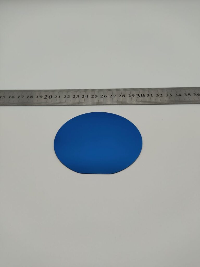
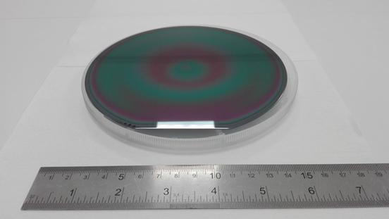
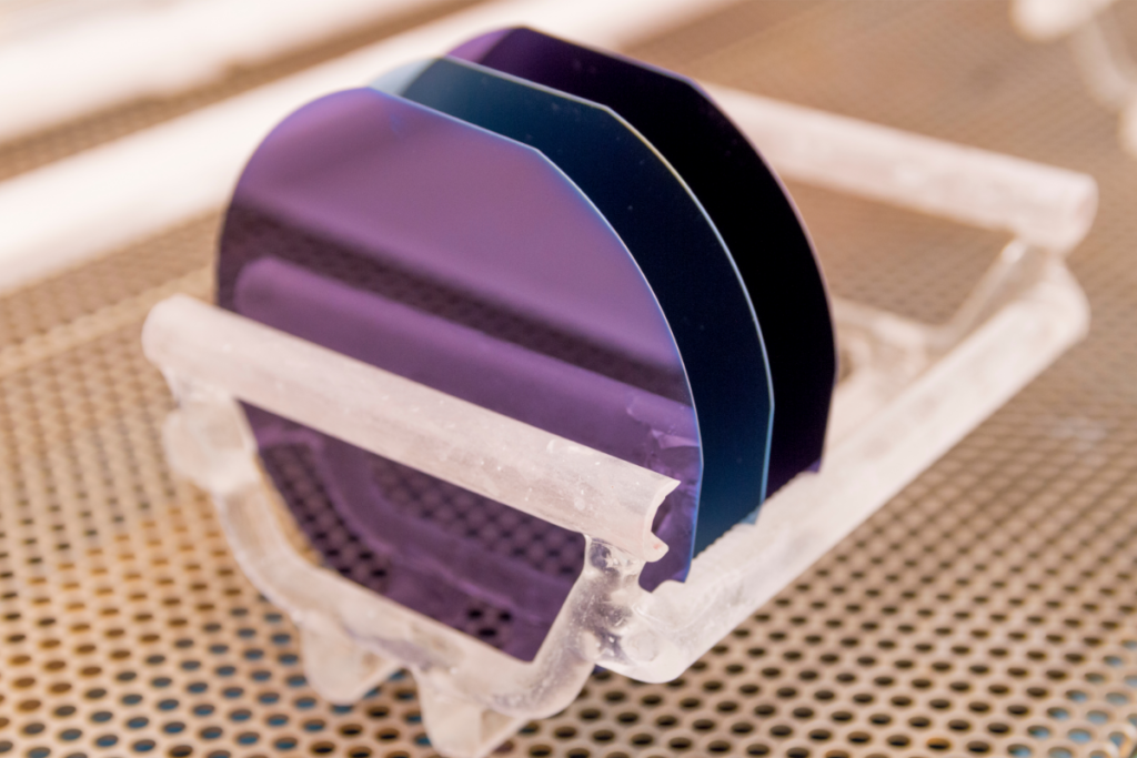
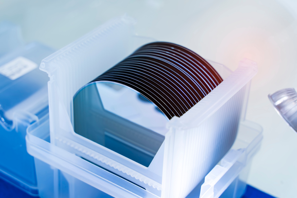
Semiconductor Crystals And Substrates
- SiC – Silicon Carbide Wafer
- Al2O3 – Sapphire Wafer
- GaAs – Gallium Arsenide Wafer
- InP – Indium Phosphide Wafer
- Ge – Germanium Wafer
- Si – Silicon Wafer
- SOI – Silicon on Insulator Wafer
- TOX – Thermal Oxide Layer on Si Wafer
- Free Standing GaN – Gallium Nitride Wafer
- Free Standing AlN – Aluminium Nitride Wafer